The Centre provides a microfabrication and prototyping facility, housed at Imperial (South Kensington and White City campuses) for the rapid production of small devices for pre-clinical in vitro studies. Supported by dedicated technicians, the facility has access to clean room facilities and a range of equipment for the development of bespoke devices. This includes 3D printing, laser cutting, electronics and access to an SU8 system for the mask free production of polydimethylsiloxane (PDMS) multilayer devices at 2-micron resolution. The facility can be used for the production of, for example, microfluidic devices, organs-on-chip, biosensors, electrochemical sensors, microneedles and others. 


Microfabrication & Prototyping for Biology and Medical Research


Microscale platforms including lab-on-chip, organ-on-chip and tumour-on-chip devices provide superior physiological environments for studying cancer biology and developing therapies. The CRUK Microfabrication & Prototyping Facility offers microfabrication techniques that have been used effectively in the areas of organoids, organ-on-chip devices and interfacing with animal models.
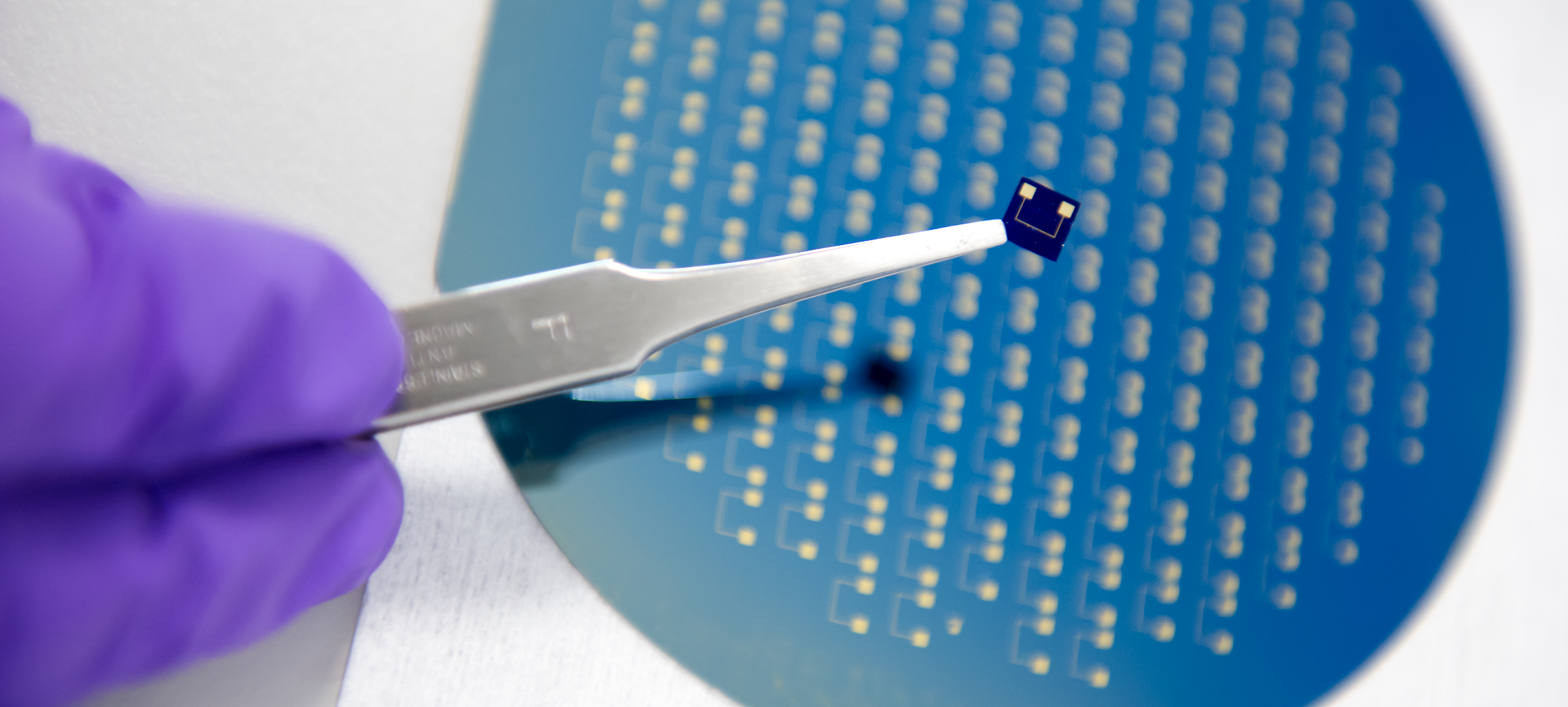
Silicon wafer in the background and three individual silicon chips held by the tweezer. The chips are nanopore sensors which are used for single protein and DNA detection.


What is available?


The facility offers its microfabrication and prototyping services in two packages, which differ based on whether the customer requires fabrication of PDMS microchips. The fabrication process of the required SU-8 devices/micro-mold and consequently the PDMS microchips will define the scope of the selected package. Hence, the cost and timeline of the requested package is dependent upon the nature of the project.


  • Single Layer Photolithography of an Existing Design
In this service, the facility will fabricate the SU-8 devices/micro-molds based on an existing photomask or 2D bitmap of an existing design. The highest resolution that the facility can guarantee is 5μm. The thickness accuracy is ±10% of the requested thickness with a minimum of 5μm and a maximum of 250 μm. The agreed cost and delivery time will depend on the type of UV printing (i.e., using a photomask or maskless UV printing), the thickness, and the type of wafer you are requesting. The offered cost includes the cost of consumables.


  • Single Layer Photolithography and PDMS Microchip fabrication of an Existing Design
In this service, the facility will fabricate the SU-8 devices/micro-mold and PDMS micro-chips based on an existing photomask or 2D bitmap of an existing design. The highest resolution that the facility can guarantee is 5μm. The thickness accuracy is ±10% of the requested thickness with a minimum of 5μm and a maximum of 250 μm. The agreed cost and delivery time will directly depend on the type of UV printing (i.e., using a photomask or maskless UV printing), the thickness, and the type of wafer you request. The offered cost includes the cost of consumables.


  • Design and Consultancy
The facility offers further expertise in the field of micro/nanotechnology and biotechnology including conceptualization, modelling, device design, and device prototyping. The details of the service will be defined upon the customer request.


Why use microfluidics in your research?


  • Significant cost savings due to smaller sample sizes and reagent volume requirements
  • The ability to closely mimic a cell's natural microenvironment
  • Multiple analytes can be processed simultaneously
  • Ideal for highly automated processes


How to use microfluidics in your research ?


By fabricating Lab on chip devices using SU 8 photoresist Microfabrication techniques to fabricate micro mold for printing PDMS based microchips.


Individual Training and Group Workshops (up to 5 persons):


The facility offers its services for individual training or group workshop for microfabrication and prototyping. The packages are divided into one- and two-day training. The price of each package includes the cost of consumables and facility reservations.


  • One Day Hands-on Training of Photolithography: This training covers the basics of photolithography and fabrication of a single layer SU-8 device, including:
    • Why photolithography and its principles
    • Learning about common defects in photolithography and possible ways to minimize them
    • How to fabricate SU-8 micro-chips on a silicon wafer
  • One Day Hands-on Training of PDMS Fabrication: This training covers the basics of fabrication of PDMS chips, including
    • A general description of the technology and its applications
    • How to fabricate the PDMS chips
  • Two Days Hands-on Training of Photolithography and PDMS Casting: Day one training covers the basics of photolithography and fabrication of a single layer SU-8 device, including:
    • Why photolithography and its principles
    • Learning about common defects in photolithography and possible ways to minimize them
    • How to fabricate SU-8 micro-chips on a silicon wafer


  • Day two covers the basics of fabrication of PDMS chips, including
    • A general description of the technology and its applications
    • How to fabricate the PDMS chips

How to access the facility?


The facility will provide training for researchers undertaking device fabrication for the first time. Access to the facility will be on a competitive basis with requests for project proposals made throughout the year with timings dependent on capacity. As with all Convergence Science Centre funding, proposals must be from cross-institution collaborative teams and use engineering/physical sciences expertise to address research or clinical questions in cancer.


Documentation:
Contacts:

For enquiries, please contact Sam Au (s.au@imperial.ac.uk) or Shahrzad Forouzanfar (s.forouzanfar@imperial.ac.uk).


You can also submit a short project proposal to icr-imperial-convergence.centre@imperial.ac.uk.